Contact Your NewwaySMTC Representative Now! [email protected]
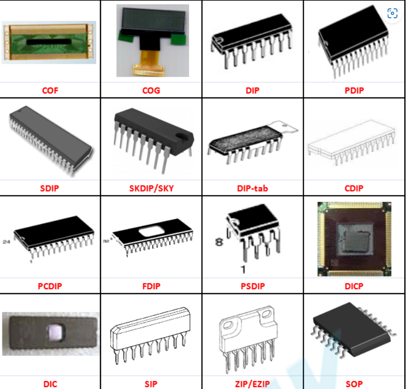
A complete list of common IC packaging tube package
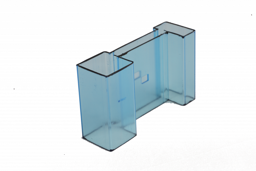
IC packaging tube package, not only plays a role in the installation, fixation, sealing, protection of the chip and enhance the electrical and thermal properties, but also through the contact on the chip with wires connected to the package shell pins, these pins are connected to other devices through the printed circuit board wires, so as to achieve the connection between the internal chip and the external circuit. Because the chip must be isolated from the outside world to prevent the corrosion of impurities in the air on the chip circuit and cause a decline in electrical performance.
What is called IC packaging tube package
In the work, often encounter various forms of packaging IC. IC packaging tube packaging, refers to the circuit pins on the silicon wafer, using wires to the external connector, in order to connect with other devices. The more advanced a chip packaging technology is measured by the ratio of the chip area to the packaging area, the closer the ratio is to 1, the better the IC packaging tube packaging chip is also easier to install and transport. As the packaging technology also directly affects the performance of the chip itself and its connection to the PCB (printed circuit board) design and manufacturing, so it is critical.
IC packaging tube packaging when the main factors to consider
- the ratio of chip area to package area to improve the efficiency of the package, as close as possible to 1: 1.
- the pins should be as short as possible to reduce the delay, the distance between the pins as far as possible to ensure that they do not interfere with each other and improve performance.
- based on the requirements of heat dissipation, the thinner the package, the better.
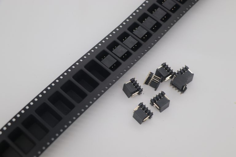
IC packaging tube package is mainly divided into two kinds of DIP double inline and SMD chip package. From the structure, the IC packaging tube package has experienced the development of the earliest transistor TO (such as TO-89, TO92) package to a double inline package, followed by the development of PHILIP company SOP small form factor package, and then gradually derived SOJ (J-type pin small form factor package), TSOP (thin small form factor package), VSOP (very small form factor package), SSOP (reduced SOP), TSSOP (small form factor package). (reduced SOP), TSSOP (thin reduced SOP) and SOT (small form factor transistor), SOIC (small form factor integrated circuit), etc. From the material medium, including metal, ceramic, plastic, plastic, many high-intensity working conditions demanded by the circuit such as military and aerospace level still have a large number of metal packaging.
IC packaging tube package has roughly gone through the following development process
Structure: TO->DIP->PLCC->QFP->BGA->CSP.
Material: metal, ceramic -> ceramic, plastic -> plastic.
Pin shape: long-lead straight insert -> short-lead or leadless mount -> ball bumps.
Assembly mode: through-hole cartridge -> surface assembly -> direct mounting
IC packaging tube packaging form
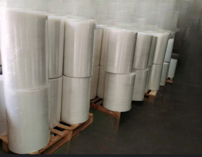
Common IC packaging tube packaging materials are: plastic, ceramic, glass, metal, etc., now the basic use of plastic packaging.
According to the package form: ordinary double inline, ordinary single inline, small double flat, small four flat, round metal, volume of thick film circuit, etc.
SOP / SOIC package
SOP is the abbreviation of English Small Outline Package, that is, small outline package, SOP package technology was developed successfully by Philips in 1968-1969, then gradually derived SOJ (J-type pin small outline package), TSOP (thin small outline package), VSOP (very small outline package), SSOP (reduced SOP), TSSOP (thin reduced SOP) (thin reduced SOP) and SOT (small form factor transistor), SOIC (small form factor integrated circuit), etc.
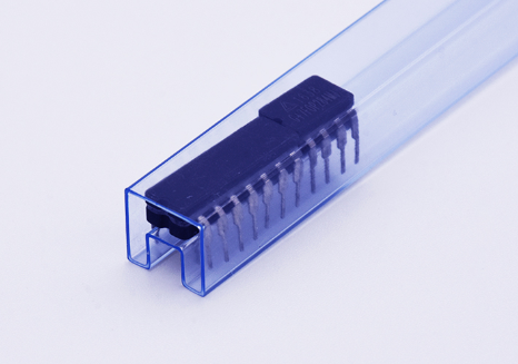
DIP package
DIP is the abbreviation of English Double In-line Package, that is, double in-line package. DIP is one of the most popular cartridge package, the application range includes standard logic IC, memory LSI, microcomputer circuits, etc.
PLCC package
PLCC is the abbreviation of Plastic Leaded Chip Carrier, that is, plastic J-lead chip package. PLCC package, the shape is square, 32-pin package, surrounded by pins, the form factor is much smaller than the DIP package. The advantages of small form factor and high reliability.
TQFP package
TQFP is the abbreviation of thin quad flat package, that is, thin plastic sealed quad flat package. The thin quad flat package (TQFP) process makes efficient use of space, thereby reducing the size of the printed circuit board space requirements. Due to the reduced height and size, this package process is ideal for space-critical applications such as PCMCIA cards and networking devices. Almost all of ALTERA’s CPLD/FPGAs are available in TQFP packages.
PQFP Package
PQFP is the abbreviation of Plastic Quad Flat Package, the distance between the pins of the chip in PQFP package is very small and the pins are very thin, generally large-scale or super large-scale integrated circuits use this package form, the number of pins is generally above 100.
TSOP package
TSOP is the abbreviation of English Thin Small Outline Package, that is, thin small size package. a typical feature of TSOP memory packaging technology is to make pins around the package chip, TSOP is suitable for SMT technology (surface mount technology) in the PCB (printed circuit board) to install wiring. TSOP package form factor, parasitic parameters ( The TSOP package form factor, parasitic parameters (output voltage disturbance caused by large changes in current) are reduced, suitable for high frequency applications, easier to operate, and more reliable.
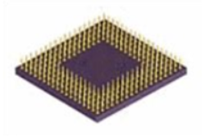
BGA package
BGA is the abbreviation of English Ball Grid Array Package, that is, ball grid array package. 20s, 90s with the progress of technology, chip integration continues to improve, the number of I/O pins increased sharply, power consumption also increased, the requirements of integrated circuit packaging is also more stringent. In order to meet the development needs, BGA packages began to be used in production.
Memory packaged with BGA technology can increase memory capacity by two to three times with the same volume of memory. BGA has a smaller size, better thermal performance and electrical performance compared to TSOP. BGA packaging technology has led to a significant increase in storage capacity per square inch, and memory products using BGA packaging technology are only one-third the size of TSOP packaging for the same capacity. In addition, the BGA packaging method has a faster and more efficient way to dissipate heat than the traditional TSOP packaging method.
The advantages of BGA technology are that although the number of I/O pins has increased, the pin spacing has increased instead of decreasing, thus improving the assembly yield; although its power consumption has increased, BGA can be soldered with the controlled collapse chip method, thus improving its electrical and thermal performance; the thickness and weight have been reduced compared to the previous packaging The thickness and weight are reduced compared with previous packaging technology; parasitic parameters are reduced, the signal transmission delay is small, and the frequency of use is greatly improved; the assembly can be soldered with a common surface and is highly reliable.
The importance of the chip is self-evident, if the lack of chips, cell phones, computers, robots and many other electronic devices will not be able to operate, which reflects the benefits of IC packaging tube packaging.