Contact Your NewwaySMTC Representative Now! [email protected]
Automatic carrier tape soldering and IC package interconnection
In IC package interconnects, the connection between the chip and the leadframe (substrate) provides the circuit connection for the distribution of power and signals. There are three ways to achieve the internal connection, namely lead bonding, automatic carrier tape soldering, and flip-flop soldering. Today, then, we are mainly interested in automatic carrier tape soldering.
What are the features of carrier tape auto soldering technology
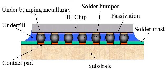
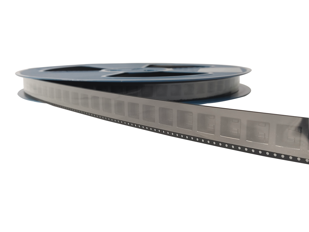
Automatic carrier tape soldering is an integrated circuit packaging technology based on the assembly of chips on a metallized flexible polymer carrier tape. The process is to form a bump on the chip, and then the bump on the chip is automatically bonded to the solder joint on the carrier tape by a lead press welder, and then the chip is sealed and protected. The carrier tape is used both as a support for the chip and as a lead to connect the chip to the surrounding circuitry, and is a metalized film.
Automatic carrier tape soldering using TAB technology for IC chip packaging has the following characteristics
(1) TAB technology can be used to form ultra-thin, small form factor devices, the thickness of which can be 0.4mm, while it has good toughness, using TAB technology to package the device on the substrate occupies an area of 10.6% of the traditional packaging devices.
(2) Automatic carrier tape soldering using TAB technology can achieve high density input/output (I/O) pins.
(3) Automatic carrier tape soldering using TAB technology improves the electrical performance of the device. Due to its flat package feature, the lead distance is shortened, and flat rectangular cross-section leads are used instead of traditional round leads, resulting in a significant reduction in interline capacitance and parasitic inductance.
(4) Automatic soldering of the carrier tape improves the thermal conductivity and increases the heat dissipation performance of the device.
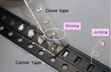
(5) The devices on the carrier tape can be transferred in a chain, which is more suitable for automated assembly. The inspection process can also be carried out continuously and automatically, facilitating early rejection of failed devices, thus saving assembly materials, improving assembly efficiency, and significantly reducing overall machine costs.
What is the automatic carrier tape soldering process – Inner lead bonding
Automatic carrier tape soldering technology includes Inner Lead Bonding (ILB) and Outer Lead Bonding (OLB). Inner Lead Bonding is a technology that interconnects the inner lead of the carrier tape with the chip bump; Outer Lead Bonding is a technology that interconnects the outer lead of the carrier tape with the shell or substrate solder area.
Automatic tape bonding for inner lead bonding
Automatic tape bonding of inner leads is usually done by hot press welding. The soldering tool is a hot electrode made of hard metal or diamond.
The bonding of the inner leads is performed at a temperature of 300 to 400°C. It takes about 1s to complete a bond.
(1) Wafer alignment. The large wafers with adhesive layers are tested and recorded, scribed into small IC wafers by an abrasive wheel scriber, and placed on the bearing table of the inner lead press welder. The IC wafer with good performance is placed under the carrier lead pattern wound on the two chain gears according to the designed soldering procedure, so that the carrier lead pattern is precisely aligned to the chip bumps.
(2) Thermocompression bonding. Drop the heated hot-pressure solder head and apply pressure for a certain time.
(3) Raise the hot press head. The soldering machine winds the IC wafer pressed onto the carrier tape onto the spool by stepping through the chain teeth, while the next carrier tape pattern is stepped to the solder alignment position.
After the bonding of the pins to the IC wafer on the reel is completed, the mating surface of the pins or the entire IC wafer inside the automatic tape soldering must be coated with a layer of polymer adhesive to protect the pins, bumps and wafers from external pressure, vibration, water vapor penetration and other factors that can cause damage. Epoxy resin and silicone resin are the most common sealing materials used by TAB.
Carrier tape automatic soldering outer lead bonding is done by using an electric frame type soldering iron tool (also called hot electrode) to press the Cu foil leads on the carrier tape into the solder metal, providing the iron with a pulse voltage that can last for a few seconds, and using the heat to interconnect the Cu foil with the solder area of the substrate.